(incomplete list)
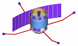
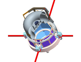
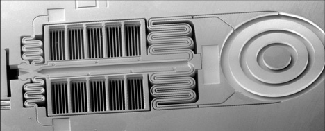
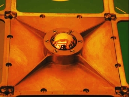
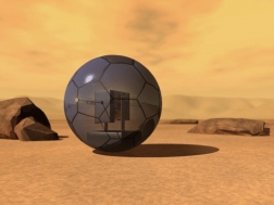
NanoSpace-1 satellite
Nanosatellites are spacecraft with a wet mass of 1–10 kg. For their functionality
to be comparable with, but not necessarily competitive to, the larger spacecraft, MEMS
technology is essential. The NanoSpace-1 was proposed and further developed beyond
phase B by ĹSTC. The main objective was to demonstrate the massive implementation of
MEMS-based system, for example, attitude and orbit control, communication, thermal
management. Even purely structural functions, such as the rigidity of the vehicle's chassis,
were maintained by MEMS materials and subsystems. NanoSpace-1 was also meant to be a space
platform of high performance, open for interfacing of heavily miniaturized payloads.
This large undertaking was broken up into major projects to develop a cold/hot gas
propulsion system for attitude control, a mono-/bi-fuel engine (“kickmotor”) for
orbit control, Multifunctional Micro/Nano systems for satellites (MMNS). Each major
project embraced a number of subprojects aiming to develop stand-alone systems, such as
a Communication Module with Thermal Management Function, a Sun Sensor, a Position Sensitive
Detector Module for docking, a Power Conditioning Module, etc., applicable to nanosatellites
in general.
The development of Nanospace-1 also created a number of
spin-off companies.
Reports from Phase A and B containing comprehensive information on
this project can be found at ESA and ĹSTC.
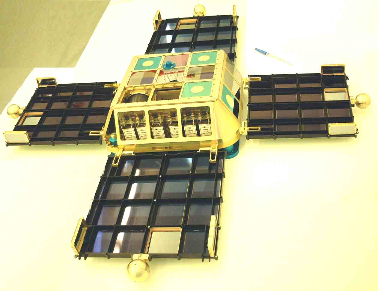 NanoSpace-1 satellite. |
Venus exploration – LOVEcraft
Space missions proposed from different nations articulate interest in Venus
exploration in general, and atmospheric investigations in particular. Development
of MEMS, and advanced materials systems are something of just-in-time solutions
for such challenging tasks, since Venus has a hostile atmosphere with
acidic gas, high pressure and high temperature. ĹSTC proposed an exploration
mission using balloon aerobot vehicles, called LOVECraft, built of durable
materials, and extremely miniaturized and multifunctional systems. The scientific
objectives of the mission were: atmosphere characterization, astrobiology
assessment, and geological investigation. The LOVECraft was designed to be a
highperformance platform for a long-duration exploration of, specifically, the lower
cloud layers. The entry unit of 30 kg would be inserted into the entry path using
a parachute. When reaching the right height the parachute would be released, a
helium balloon carrying a gondola would deploy, and a lander with a now empty tank
would be released. The balloon with the gondola containing 20 active ballast
probes for surface investigation would continue is journey above the ground for
1-6 month to cover a vast area of Venus. A feasibility study, and a mission and
design outline have been made in this project.
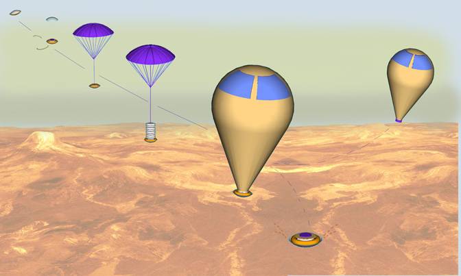 Insert sequence of the entry unit into the Venus atmosphere. |
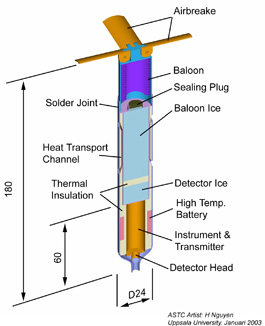 Balast probe in cut view. |
Earth intelligent surveillance
Short Earth surveillance missions of very varying nature asked for the development of a
small and flexible satellite systems. The Earth Intelligent Surveillance (EIS) mission,
proposed to the Swedish Armed Forces by ĹSTC, was developed beyond phase 0, and
the system, including structural design, propulsion, attitude control, and payloads
was drawn up in detail. This satellite with a wet mass of about 27 kg employed
mainly MEMS modules and systems developed for NanoSpace-1 and a
high resolution camera, and was aimed for quick preparation and air launch independently
of the weather condition. A number of research subprojects was generated, such as a
MEMS-based system for propellant measuring, a new type of flexible solar panels, and
a new structural concept, to name a few.
 The Earth Intelligent Surveillance satellite |
 Cut view showing the structural design of the satellite. |
NSWS
(Information on this project is comming soon.)
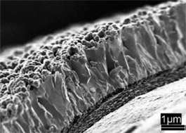
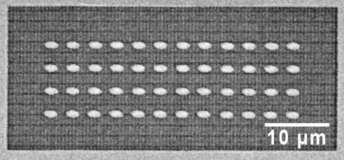
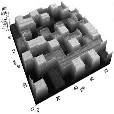
MEMS filter
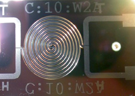
Microfluidic systems for cold gas propulsion on the satellite NanoSpace-1
and EIS require a gas flow free from particles that can
clog the narrow passages measuring down to few micrometres. The most vulnerable
parts are microvalves. Particles can be generated from in-orbit-activation of the
cold gas propulsion system or can simply be contained in the storage tank from
the begining. ĹSTC developed a 3-D filter, which stops particles with diameter
larger than one micrometre from entering the microfluidic systems, and which can
operate throughout the mission duration. Simulations and measurement of the flow and
the pressure drop in the filters manufactured from silicon showed that the
concept worked well. This also resulted in a design rule for V-groove
silicon-based MEMS filters. The 3-D filter became a generic component in many of
the microfluidic cold gas systems and devices developed at ĹSTC.
The mentioned design rule, wich might be the most interesting outcome from this
project, can be found in J. Micromech. Microeng. 16 (2006) pp. 2006-13.
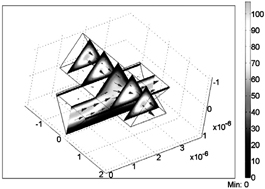 Finite element analysis of flow in crossed v-groove junction. |
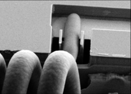
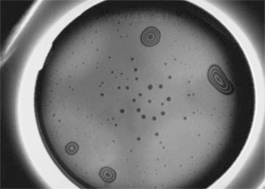
Thrust balance
In order to measure the reaction force from a cold gas thruster or
microrocket of a few micro Newton, an instrument called Thrust Balance
was built and placed in a vacuum chamber. The Thrust Balance consists of a framework stand
in which a pendulum is hung freely on two strips of thin foil of stainless steel. A highly
sensitive position sensor is placed on the bottom plate of the stand to measure the
displacement of the pendulum as the result of the reaction force when the thruster is
activated. An electromagnetic coil gets a voltage from the close-loop feedback electronic
system to counter-react the pendulum displacement.
The vacuum chamber is composed of a main chamber connected to a tubular chamber. The main
chamber has a glass dome allowing for monitoring during measurement, and three ports allowing
for mounting of the thruster and service of the equipment. The glass dome can be electrically
lifted to open the main chamber from the top in case the Thrust Balance needs to be lifted.
The tubular chamber functions as the empty space allowing for the plume of gas from the
thruster to develop freely.
The measurement system has been used until the design of the cold gas thruster was changed,
and the system for sensing of the reaction force of the cold gas nozzle was integrated into
the thruster.
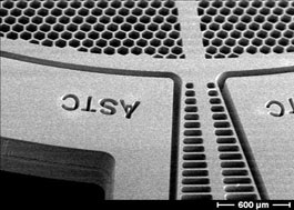
Structural module for nanosatellites
Because MEMS is massively implemented in the nanosatellite in order to increase the number
of systems and function per mass and area unit of it, silicon is an abundant material onboard.
With the modular approach to the spacecraft design, most of this is accommodated in the form
of flat panels forming an essential part of the vehicle´s chassis. Four-inch wafers were
chosen to be the standard substrate due to the available clean room equipment. From these
wafers, 68x68 mm square panels with processed devices were cut out. For mounting and interfacing
of the panels 74.6x74.6x7.5 mm aluminium frames were developed. The aluminium frame is a mechanical
protection for the MEMS module, which normally is a stack of several structured
silicon wafers bonded together. The aluminium frame also provides reference surfaces and screw
holes for mounting onto the satellite.
The brittle silicon stack requires a special interface to the relatively elastic aluminium
frame. A thermally conductive silicone rubber was used to mount the silicon stack in the frame
through a casting process, where sidewalls of the frame and the silicon stack were parts of the
casting form. A special Teflon fixture was used to position the stack accurately inside the frame.
Finite element analysis and mechanical tests were performed, and the results showed that the modules in
their aluminium frames can be used as structural element in nanosatellites.
The investigation is presented in J. of Spacecraft and Rockets (43) 6, pp 1319-27. (only first page provided)
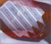
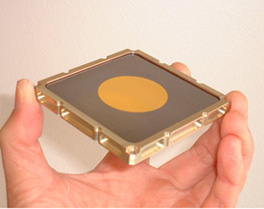 Framed communication panel. |
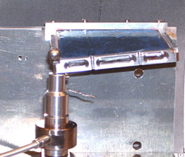 Destructive bending test showing framed dummy wafer prior to fracturing. |
Micro o macro
(Information on this project is comming soon.)
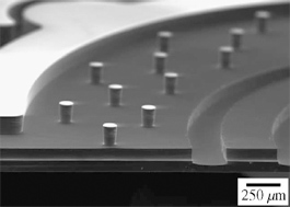
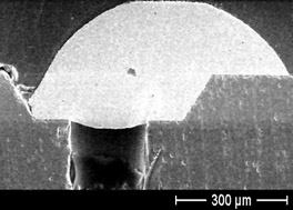
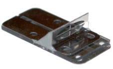
Paraffin-based gas valve
As part of a main valve to control the gas supply to the thruster pod in the cold gas system, meander-suspended
and caddy-shaped thermal actuators were investigated here. By using corrugated diaphragms for the paraffin-filled caddies’
top and bottom the actuators could be tailored to expand more or less linearly with the internal pressure caused by melting
of the paraffin wax.
The devices were made by fusion bonding of silicon wafers structured in three steps by deep reactive etching, followed by
dicing. In this prototype phase, heat was supplied through external flexfoil heaters.
Because of difficulties to control the amount of paraffin charged into the caddies, their membranes typically experienced
an initial inward deflection of a few micrometers when the wax had solidified. On full melting of the wax, an outward
deflection of about 10 micrometers could be observed.
For mechanical testing of empty caddies, a load increasing up to approx. 4 N was applied to the 1.5 mm diameter non-corrugated
center of the diaphragms via a ball point probe. All devices responded to this by deflecting, the weakest members by close
to 90 micrometers, the stiffest ones by 50.
To increase the response time of the actuators, a few samples were equipped with silicon fingers on the inside of the caddies
to better facilitate heat transfer from the enclosing silicon. However, as a means to speed up the device, this just affected
the very first seconds of the deflection curve, and this at the cost of a few percent less stroke.
Details are given in Sensors and Actuators A105, pp. 237-46, 2003.
 Valve operation principle. |
 Inside of caddy lid half way through processing showing heat fingers. |
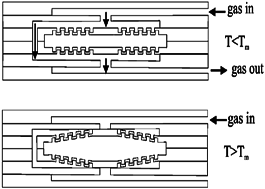
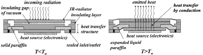
Thermal switch
Orbiting spacecraft are often subjected to fluctuating temperatures, both because of changes in incoming radiation, but also
because of changes in internally generated heat. Small, shell-based satellites are particularly prone to this.
In this project, a thermal switch the size of a full panel (68x68 mm) of the NS-1 satellite was designed, built, and
evaluated.
A number of silicon wafers processed by deep reactive ion etching and wet etching to contain ring-shaped membranes of various
diameters, were joined into a stack forming a ring-shaped cavity between two of the wafers. Filled with paraffin wax, and
sealed, this cavity expanded on reaching the melting point of the wax, in such a way that the center part of the system
deflected and closed an otherwise insulating gap to an IR-emitting member of the device.
The six switches manufactured and studied, all showed a sudden deflection of approximately 90 micrometers (i.e. about 10%
of the device thickness) at the phase transition of the paraffin. This deflection was found to decrease linearly when a load
of up to about 3 N was applied to the deflecting part. One device was mechanically tested until it fractured at 13 N.
In general, the performance behaved as planned, but some weaknesses were found. For instance, the center part, intended to
traverse the insulating gap and make good thermal contact with the heat emitting wafer, was too weak and lost its flatness
upon actuation. Also, non-uniform heating and cooling lead to an inclination of the center part.
Further details are given in Sensors and Actuators A96, pp. 189-95, 2002.
Actuator part of the thermal switch device.
 |
| Working principle of thermal switch in cross section. |
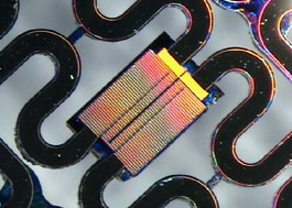
Piezoelectric gas flow valve
A predecessor to the design with paraffin-based valve for the cold gas hybrid thrusters, was a low-power piezoactuator
consisting of five multilayered piezoceramic (PZT) legs around the valve cap, and a single ceramic leg on the cap itself.
Integrated in a silicon part bridging all six elements was a strain sensor to monitor the contact pressure between the valve
cap and its seat. The working principle was to extend the peripheral legs and contract the centre one to open the valve.
Among the benefits was close to thermal indifference, wear resistant contact surfaces, and a good precision in the closing
and opening of the valve because of the dual actuation.
Fabrication, however, proved to be difficult, especially the thin-film soldering of the ceramics to the silicon substrate.
Without careful control of the thicknesses of the metallizations and solder layer, the strength and yield were reduced.
At its best the structures exhibited a leak rate below 1E-6 scc/s He.
 Fluid control chip with two piezoceramic valves. |
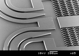
Cold gas propulsion
Many are the activities carried out in the group to study and develop cold gas thrusters, whereto also heated (hot) cold gas
systems count. For the nanosatellite, these thrusters play a key role for the attitude control.
Basically, the cold gas system is just a means of dispensing gas in a controlled way and benefit from the reaction force.
Needless to say, miniaturization of the last parts, i.e. final valve, stagnation channel and nozzle of the system, should
enable a more precise dispensing. To make more efficient use of the propellant, is another issue.
In the rocket chips designed, manufactured and tested at the ĹSTC, the channel widths are around 100 micrometers and the
entire chip about as large as a small finger nail. Such small dimensions demand close to particle-free gases wherefore a
reliable and finely structured filter became an important part. A couple of valves, a few flow meters, and
means to use force feedback (not presented here) have also been studied.
An interesting part of the cold gas program was the development of heaters to be placed just before the nozzle in order to
gain efficiency. Tremendous efforts were spent on building fully 3-D heating coils from diamond-like carbon by precipitating
the material out of thin air, so to speak, by a focused laser. Theses heaters were then mounted and fixated in the
channel by clamping combined with soldering or focused ion beam deposition.
Heaters were also made similar to the ones for the flow restrictor with silicon lamellas transferring heat evenly into
the gas flow.
An overview of the cold gas thruster program with components examples are given in the summary of J. Bejhed’s thesis summary.
 |
| Half a microrocket chip with nozzle to the left and a valve seat to the right. Six little notches along the mid channel contain clamps for coil-shaped heaters. |
 Close up of heater mounted in clamp. |
 Different nozzle design with amella heaters. |
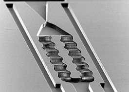
Kick motor
A motor completely different from the cold gas system – in both purpose and principle is the monopropellant micro-kick motor.
Mounted on the top of the NanoSpace satellite, this motor is intended for orbit maneuvers, not for attitude control.
The heart of the motor, and, in addition, the most finely structured part of the system, is the monopropellant decomposition
chamber with a stack of suspended catalyst beds made of silver-coated silicon shaped into honeycomb structures by deep reactive
ion etching. This clamped stack is equipped with a boron nitride nozzle on top and stands on four pipe legs (two for the fuel
and two for electric lines and pressure feedback) connecting it to fluid handling module inside the spacecraft.
This project posed many challenges. A particular one was the interfacing of the metal pipes with silicon.
With hydrogen peroxide as monopropellant, the anticipated thrust was 20-200 mN, and the specific impulse 100-150 s.
The prototype was developed together with QinetiQ, Surrey Satellite Technologies Ltd (UK), and TNO (ND) under an ESA contract.
 Kick motor with nozzle on top. |
 Part of catalytic bed. |
Solder sealing
The group’s many devices based on the heat-induced expansion of paraffin wax, for a long time shared the problem of sealing.
The reservoirs are usually filled with liquid paraffin which tends to wet the surfaces far outside the interior ones preventing
the use of adhesives. In addition, a thermal sealing method applied to miniaturized systems would at least threaten to melt most
of the paraffin charge and cause a loss of material as well as expansion/stroke.
A solution to this is the solder sealing method where the device, now equipped with an integrated heater close to the inlet to
the paraffin reservoir, and coated with a metal thin film around the very orrifice, is filled as usually and cooled down to
solidify the wax. Without any concern about wax contaminants, a small amount of solder paste is then dispensed or screen printed
above the more or less paraffin-blocked opening. Upon heating the opening very locally through the integrated thin film heater,
the paraffin residues melt, and the solder particles sink through and solders to the opening metallization, sealing the system
with a minimum of paraffin losses.
In the first exploratory study, attention was paid mainly to the heating cycle and the dependence of sealing performance on the
alignment of the metallization. Evaluation was made by microscopy, and leak testing at 85şC with nitrogen at 8 bar for eight hours.
The results indicated that the paraffin was successfully driven away from the surface by the solder creating a clean interface of
good adhesion. The process was found to be rather forgiving with respect to misalignment of the pad around the orifice, but a
combination of misalignment and intense or prolonged heating skewed the solder bump to one side. Excessive heating also seemed to
lead to a consumption of the metallization causing the pad and footprint of the solder bump shrink. In conclusion, the process was
very robust and straightforward.
Further information is given in J. of Micromech. and Microeng. 16(11), pp. 2369-74, 2006.
 Inverted mesa orifice with part of meandering heater. |
 Cross section of sealing with solder bump (white). |
Laser assisted chemical vapor deposition
Laser assisted chemical vapor deposition (LCVD) is one of rather few microtechnologies which allow for fully 3-D freedom. By
focusing a laser beam on a substrate placed in a chamber with reactive gases a solid deposit will form in, and close to, the beam
spot. Then, by moving the point of focus and the substrate with respect to each other at a speed corresponding to the rate of
deposition, a structure is more or less freely drawn.
The more generic work done by ĹSTC in this field involved the investigation of shape, morphology, and mechanical properties as
functions of process conditions (i.e., laser power, ethylene partial pressure, and translation speed). Soon, also operational
tests were conducted to see how the material in the form of microhelices (coils) would endure the intended application – working
as electrically driven heaters in the stagnation channel of (heated) cold gas thrusters to increase the specific impulse for a
given amount of propellant.
The first attempts with carbon structures for this application resulted in extensive erosion even when operated in an inert gas,
wherefore coating with Tungsten was included in the manufacturing scheme. This improved the endurance of the heaters significantly.
As for the generic studies, it was at first difficult to see a well-behaved relation between the modulus of elasticity and the
pressure and laser power. Cross-sectional microscopy, however, revealed that the structures consisted of up to three morphological
zones. These zones – all of different stiffness – could be related to the temperature distribution in the deposit during processing.
More information can be sought in Carbon, 45(3), pp. 484-492 (2007).
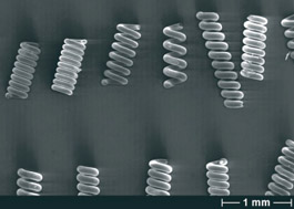 Various LCVD manufactured coils. |
 Cross section showing tungsten coating. |
Bond strength characterization
Often, assembling by bonding structured wafers together is the way to achieve fully three-dimensional systems with the otherwise
planar processes employed in microtechnology. Usually a strong silicon-to-silicon bond is attained by carefully cleaning, putting
together, and annealing flat and polished wafers.
As with all non-ductile materials, the strength of the bond as well as the bulk material is governed by the weakest parts –
usually voids, sharp edges and impurities. Therefore, a good understanding of the mechanical reliability of bonded silicon
structures can be obtained from statistical analysis of test data.
In a long series of bond-related studies, it was found, for instance, that:
- Weibull statistics provides a good tool for analysis of blister test data, especially if great care was taken to clamp the
samples rigidly to minimize effects from the fixture,
- applied to anodic bonding, the statistical model revealed the bond strength to be comparable to that of fusion bonding,
- in bonding silicon to thermally oxidized silicon, plasma treatment of the latter member significantly improved the bondstrength,
but never to the level of silicon-to-silicon bonding,
- bonds are highly resistant to spaceflight environment.
A comprehensive review on bond testing methods can be found in Materials Science and Engineering: R: Reports 50(4-5), pp. 109-165.
 |
| Bond interface from plasma-activated surfaces after annealing (IR image). |
Xenon gas flow restrictor
Besides the obvious method of limiting a gas flow by using a throttle valve, one can add heat to the gas in order to increase its
viscosity and make it more reluctant to flowing.
One ĹSTC project investigated the possibility of using this principle for a flow-control unit in a Xenon-based electric propulsion
system. The heart of the corresponding device was a heat-exchange chamber made of silicon. This chamber contained hundreds of
lamellas, in themselves reducing the flow, but also transferring heat from metal heaters deposited on the outside to the passing
gas. To confine the heat to the chamber, it was suspended in relatively long meandering arms.
The evaluation confirmed that the mass flow could be decreased by around 30% by increasing the temperature from room temperature
to about 200şC. However, it was also found that the suspension channels caused most of the overall reduction. With a new “flat coil”
design, the main restriction did come from the heat exchange part, but now the heat loss through the less insulating suspension was
too high.
 Complete flow restrictor. |
 Close up of inlet to open heat exchanger. |
 Another design for flow restrictor. |
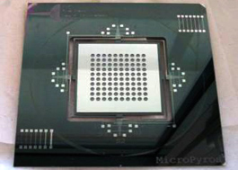
Solid propellant microrockets
Not far from the hot cold gas systems in terms of lever, there is another and completely different attitude control system for
the NanoSpace-1 satellite: the Micropyros arrays. Like the cold gas pods, these arrays are placed far out on the solar
panels. Each array consists of one hundred single-burn, solid propellant rockets, a number of which can be fired to give the
satellite a ‘digital torque’ down to a millinewton meter.
The main challenges of this project was to assemble the rockets (in particular given the temperature constraints), and to avoid
crosstalking during firing.
ĹSTC’s main part of the project was the thrust vector measurements including a theoretical analysis of vibrational modes of the
thruster chip. This included the design, manufacturing and testing of a test platform with slender suspension arms equipped with
integrated strain gauges.
 Micropyros chip in test frame. |
 Ignition testing. |
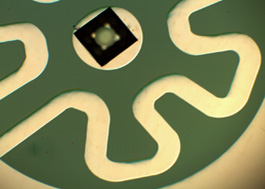
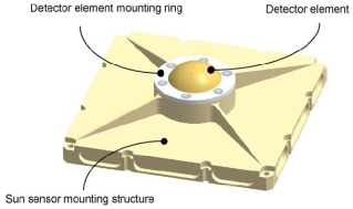
Sun sensor
It is important for a spacecraft, powered by sunlight via solar cells, to be able to point the spacecraft towards the sun.
A detector that measures the boresight angle towards the sun is called a sun sensor. A project conducted at the ĹSTC used
a novel detector design comprising a curved surface with photosensitive material. The curved surface was coated with
a thin-film photosensitive material called CIGS (copper indium/gallium diselenide).
Extensive information on the sun sensor efforts are given in the licentiate thesis summary of T. Böhnke.
 Sun sensor module in schematics. |
 Module mounted on satellite model. |
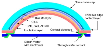 Layer structure of sensor element. |
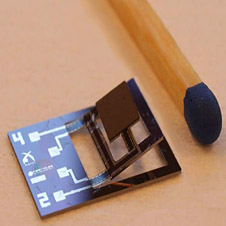
Multifunctional micro- and nano-systems
It is common in the academia and industry to study micro- and nano-systems at the device level and not on a module/system
level. One of the reasons for this device oriented view is that the manufacturing complexity increases
drastically with the module size and the amount of multifunctionality in the module/system. In the project called
Multifunctional Micro- and Nano-systems (MMNS) an attempt was made to incorporate as a thermal management function together with a
S-band transmitter/receiver in the same silicon wafer stack. The thermal management part of the module acts both as thermal
storage and a thermal switch with the usage of paraffin. In addition, paraffin was used as a low loss
microwave substrate for the antenna function of the system. All in all, the module consists of four silicon wafers and one
glass wafer.
Details are given in J. of Spacecraft and Rockets, vol. 43(6), pp. 1377-86. (only first page provided)
 Exploded view of the MMNS module. |
 Module half way through processing. |
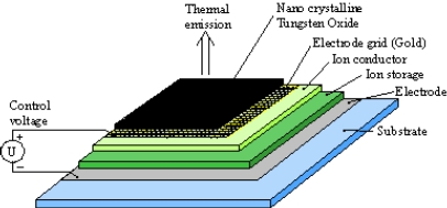
Variable emittance panels
One of the major challenges for spacecraft designers is thermal control. Several strategies exist including e.g. louvers,
radiators, and heat exchangers. These technologies are bulky and not applicable on miniaturized spacecraft. One possible
type of thermal control is optically active coatings. These can be electrically controlled to alter the reflectivity and absorption. At
the ĹSTC, an all-thin-film electrochromic device has been investigated. As illustrated below, the optical
properties of the surface can be radically changed in electrochromic devices. Electrochromic devices are a potential
solution to the thermal control challenge that exists on miniaturized spacecraft.
More information is given in Anna-Lena Larsson's thesis summary.
 |
| Layer structure of device. |
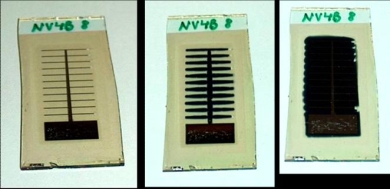 |
| Device increasingly activated to change colour and emissivity. |
Cold surfaces for spacecraft thermal control
In contrary to the common belief that space is extremely cold, it is in fact at least as big a problem that spacecraft
overheat. In space there is solar energy in the form of direct solar flux and by Earth reflected solar flux impinging
on a spacecraft. In addition, energy in the infrared region eminates from the Earth due to its temperature. All cooling of
the spacecraft is made by radiation since convection and conduction of heat away from the spacecraft is not possible. A
detailed study was conducted to find suitable coatings and microstructures, compatible with miniaturised spacecraft
technology. The basic building material was silicon, with and without microstructures, and coatings of aluminium and
silicon oxide. It was shown that the surface properties of solar reflectance and thermal emittance could be adjusted by
using microstructured surfaces with the coatings aluminium and silicon oxide.
Details are given in Optical Materials, vol. 30(9), pp. 1410-21.
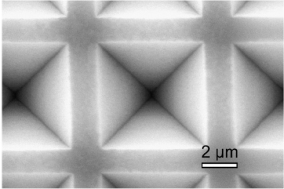 Inverted pyramids etched in silicon, rendering the surface a larger area. |
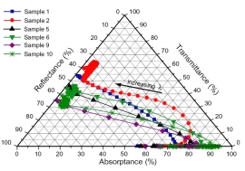 Optical parameters changing with wavelength and different coatings and surface topographies. |
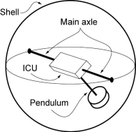
Spherical microrover for planetary exploration
A locomotion principle based on an invention of Per Samuelsson was investigated, and its potential as a microrover
studied. An inflatable spherical shell with a main axle, pendulum, and several electrical motors constitute the microrover.
The microrover was remotely controlled and the microrover was able to transverse long distances. Several microsystems were
investigated for usage onboard the microrover including a multifunctional shell with thin film solar cells,
antennas/communications configurations, integrated electronics (multi-chip modules), sun sensors, cameras, accelerometers,
and gyros. In addition, a detailed investigation of the intricate relationship between obstacle height, radius of
microrover, and centre of mass was conducted.
 |
 |
| Artist's view of rover on mission [Proc. of ISU Alumni Conference 2003]. |
Locomotion part with pendelum [Proc. of ISU Alumni Conference 2003]. |
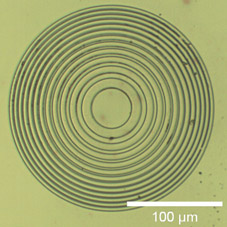
High frequency antenna and feeding networks
For several years now, antennas and feeding network systems have been manufactured by micromachining technologies.
Benefit of this are the manufacturing precision needed for high-frequency applications,
and the compatibility with semiconductor devices. On-chip antennas and flexible antennas are two examples of this. At the ĹSTC,
antennas and feeding network systems for GPS, S-band, K-band,
and W-band have been demonstrated.
 |
 |
| Stack of silicon wafers forming an antenna substrate. |
Satellite panel with electroplated patch antenna. |
 |
 |
| Loop antenna etched in silicon. (Inserts of higher magnification.) |
Wave guide based on nanowires in flexible prited circuit board. |
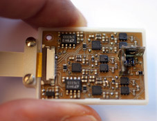
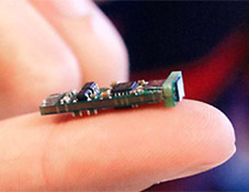
Multichip modules
A multichip module is characterized by the usage of multiple naked interconnected electronic chips packaged together. Since, in reality,
bare electronic chips are very small, much space can be saved if one can do without individual packaging,
e.g. plastic encapsulation, of the components. Instead the protection of a multichip module is provided, collectively, by the module itself.
One implementation strategy is to
mount the bare electronic chips on micromachined silicon wafer carriers and deposit interconnects using thin film
deposition, e.g. sputtering and lithography. The encapsulation of the module is provided by another silicon wafer that
is bonded onto the primary wafer (or wafers). By this, modules for spacecraft, e.g. flight computers, can be integrated into small volumes.
The use of micromachining technology enables the formation of narrow vias through
the stacked wafers. Other advantages with stacked electronics in multichip modules include reduction
of interconnect routing problems, less time delay for high speed signals, less thermal problems, and a more robust system.
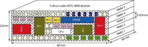
Five-wafer stack accomodating various components in schematics.
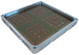
An open module revealing the chip recesses and parts of the interconnections.
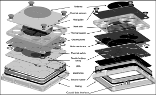
Agile Optical Communication for Formation Flying Spacecraft
Formation flying spacecraft enable a new generation of high resolution imaging and remote sensing. Characterisation of Earth-like planets is one example where formation flying spacecraft can reach the resolution needed to accomplish the scientific goals by forming a huge virtual aperture.
In this program which comprises several projects and studies, agile optical communication modules for usage on miniaturized spacecraft platforms have been investigated. Pulsed visible/infrared light was used for performance advantages with respect to power consumption, module weight, and data rate, compared with traditional RF/microwaves. Several important subsystems including electronics, optical beam steering, and lenses were designed, manufactured, and evaluated in-house.
In planned formation flying missions, a typical distance between spacecraft is 1-10 km. One of the project goals was to have a 1 Gbps data rate at these distances. A pulse-position-modulation (PPM) technique was used together with electronics including VCSEL, VCSEL driver, avalanche diode, limiting amplifier, clock and data recovery, and de/serializer. The data rate aimed for was found feasible with a laser power of 10 mW and transmitter/receiver apertures of 1 cm in diameter.
Great efforts were spent on developing the beam shaping and steering parts. In particular, the actuation platform of a mirror was studied through finitite element modeling, lumped elements modelling and, of course, prototyping and physical measurements.
Project team: Sara Lotfi, Kristoffer Palmer, Johan Sundqvist, Pär-Johan Oskarsson and Greger Thornell.
 Fresnel microlens for beam collimation. |
 Mirror device with hinge-like actuators. |
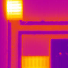 IR image of thermally actuated hinges. |
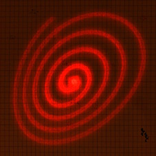 Scan pattern drawn in laboratory cealing. |
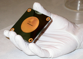
SDT Magnetometer
Magnetometers are common satellite instruments used for both attitude control and scientific measurements. The traditional magnetometers are quite bulky. Therefore the need for a new type of very small magnetometer has developed, in which mass and power consumption is minimized, making it employable on nano-satellites (länk till *NanoSpace-1 satellite*).
ĹSTC has developed a miniaturized magnetometer of a few grams, called Spin-dependent Tunneling Magnetometer (SDTM), based on the tunnelling magnetoresistance (TMR) effect. The TMR effect works much like the giant magnetoresistance effect, that was awarded the 2007 Nobel prize in Physics, and has been developed for use in hard drive read-heads and for the next generation of non-volatile magnetic random access memories (MRAM). The TMR effect employs a fixed and a free ferromagnetic film separated by an extremely thin dielectric film, or barrier. When a voltage is applied over the barrier, electrons will start to tunnel, and the electric resistance will depend on the magnetization of the ferromagnetic films via the quantum mechanical tunnelling process. If the films have parallel magnetization, the resistance over the barrier is low. Oppositely, if their magnetizations are anti-parallel, the resistance will be high. The magnetization of the free film (also called the sensing film) is dependent on the ambient field and the resistance over the barrier will therefore be dependent on the strength and direction of this field. A sensor based on the TMR effect is called a magnetic tunnel junction (MTJ) and can be used for measuring one component of the magnetic field vector. SDTM employs MTJs in an orthogonal configuration to measure the full magnetic field vector.
The main focus of the SDTM project has been to develop micro- and nano-structuring processes for fabricating MTJs. This was done using processes like Focus Ion Beam (FIB), argon ion milling among others. The structured sensors had lateral sizes ranging from 500 nm to 100 µm and were, after comprehensive analysis and characterization, incorporated with supporting electronic, also developed in-house, to form the SDTM system. Now, the process of space-qualifying the system has been started and the project is currently in the stage of seeking suitable missions to tests in space.
Project team: Anders Persson, Greger Thornell, Johan Sundqvist, Lukas Karlsson and Hugo Nguyen.
 Tunnel junctions etched with focused ion beam. |
 Second generation integrated sensor system on PCB. |
 Final, flight-ready sensor system. (Total mass: 0.7 g.) |
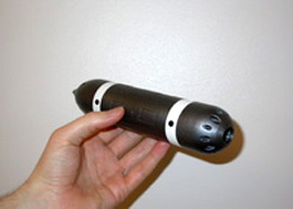
Deeper Acess, Deeper Understanding
As global warming becomes more of a concern, and environmental research increasingly important, scientist are striving to collect data in ways and places previously not possible. Also, with the current successful missions to other worlds in our solar system, the search for extreme and extraterrestrial life is an area of increasing interest.
An application combining both of these areas is the exploration of subglacial lakes, i.e. bodies of water gathering underneath glaciers and ice caps through geothermal heating and by the pressure exerted from the ice above. Some of these lakes have been sealed off from their surrounding environments for considerable periods of time and are thought to harbor a unique biota, and contain important information on how life conditions were several thousand years ago.
The DADU project was to develop a miniature submersible vehicle, which could perform distant and autonomous exploration, and analysis in harsh and narrow environments. It was designed to be able to reach down through narrow glacial bore holes and into the previously unreachable subglacial lakes, to explore and make in-situ measurements.
The vehicle is equipped with high-resolution imaging, both visually and acoustically, and sensors to measure the physical properties of such lakes. The vehicle is tethered by a several hundred meter long fiber optic cable, making real time transmission of data possible. This enables scientists to make quick in-the-field decisions of which areas are of highest scientific interest.
This vehicle will be a forerunner to future small autonomous submersible explorers, for exploration here on Earth as well as beyond, such as the global subsurface ocean thought to exist on Jupiter’s moon Europa, and more recently Saturn’s moon Enceladus.
Project members: Jonas Jonsson, Erik Edqvist, Hugo Nguyen and Greger Thornell
 |
| First model of hull and propulsion modules (from ESA's coverage). |
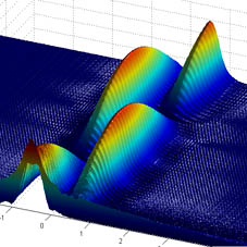
Miniaturized side-scan sonar
A miniaturized side-scan sonar was developed for the DADU vehicle to acoustically image the surroundings. Such a sonar works by sending out fan-shaped beams, through a piezoelectric element, and with the same element registering the acoustic response (echoes) from the surroundings. These beams are wide in the vertical direction and narrow in the horizontal. As the vehicle moves forward, each beam received progressively adds line after line to build up an acoustic image.
The resolution of the system is dependent on the dimension and operating frequency of the element, the larger the size and frequency, the smaller the lobe, and thus the resolution. Being restricted by the small size of the submersible, a higher operating frequency is needed for the miniaturized sonar element to adequately resolve its surroundings.
In this case, with the dimensions of the piezoelectric transducer approaching the wavelength in size, it was important to understand the interference between beam and the hull’s enclosure. This was made by finite element modeling, and measurements both in laboratory and in field.
Project members: Jonas Jonsson, Erik Edqvist, Johan Sundqvist and Greger Thornell
 Early sonar image revealing rocks, a cable and a school of fish. |
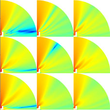 Acoustic beam modeled with various enclosure widths and heights. |
Fiber optic interface
To be able to send and receive real-time data and commands through narrow environments, where a direct line of sight is not possible, a fiber optic cable, several hundred of meters long, will connect the DADU submersible with the ground station. Through this fiber, multiple wavelengths of light will be used to simultaneous send data in both directions and even power to the submersible, to charge its batteries.
To fit the DADU application, commercial off-the-shelf components couldn’t be used. Instead the fiber optic interface needed to be tailored to its specific purpose using waveguides with evanescent wave coupling. Through this the individual wavelengths could be merged and separated at both ends of the fiber. After thorough simulation, thick waveguide polymers were deposited in several layers and patterned by means of UV lithography.
Project members: Jonas Jonsson and Greger Thornell
 Simulation of light coupling between two waveguides. |
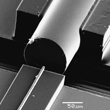 Holder of optical fiber and interface to waveguide. |
Diffractive optics for increased perspective in images
The DADU craft is equipped with a camera for real time imaging. Pictures captured with a normal camera are without perspective, which is a problem with most underwater imaging. The images tend to be flat and it is hard to convey how far away the object is, and what size and shape it has. In order to add this extra information to the pictures a well-known pattern can be projected onto the object. This pattern has to be in focus independent of the distance from the camera within a reasonable region, and therefore has to be collimated. To achieve this, a diffractive optical element (DOE) can be used, which re-shapes a laser beam into a desired fan-out pattern.
A DOE is a lens that changes the phase and/or the amplitude of the incoming beam in order to change its propagation properties, thus gives the advantage of being able to redistribute the intensity of the beam into a desired pattern.
This project involved the design, production and evaluation of several such different DOE lens prototypes, and the development of the software to handle post processing and measurements. Although field experiments were not conducted, great care was taken to mimic, e.g., turbid water and environments where organisms are attracted to the camera light.
Project members: Martin Berglund, Jonas Jonsson and Greger Thornell
 Atomic force microscope image of etched diffractive lens element. |
 Nose cone of DADU vehicle (5 cm diameter) with laser fan made visible with liquid nitrogen. |
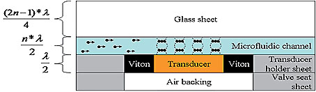
Acoustically enriching, large-depth aquatic sampler
In marine biology, it is useful to collect water samples when exploring the distribution and diversity of microbial communities in underwater environments. In order to provide, e.g., a miniature submersible explorer, like the DADU vehicle, with the capability of collecting microorganisms, a compact sample enrichment system has been developed. This sampler is 30 mm long, 15 mm wide, and just a few millimetres thick. Integrated in a multilayer steel, polyimide and glass construction is a microfluidic channel with piezoelectric transducers, where microorganism and particle samples are collected and enriched, using acoustic radiation forces for gentle and labelless trapping. High-pressure, latchable valves, using paraffin as the actuation material, at each end of the microfluidic channel keep the collected sample pristine. A funnel structure raised above the surface of the device directs water into the microfluidic channel as the vehicle propels itself or when there is a flow across its hull. The valves proved leak proof to a pressure of 2.1 MPa for 19 hours and momentary pressures of 12.5 MPa, corresponding to an ocean depth of more than 1200 metres. By reactivating the latching mechanism, small leakages through the valves could be remedied, which could thus increase the leak-less operational time. Fluorescent particles, 1.9 µm in diameter, were successfully trapped in the microfluidic channel at flow rates up to 15 µl/min, corresponding to an 18.5 cm/s external flow rate of the sampler. In addition, liquidsuspended GFP-marked yeast cells were successfully trapped.
Project members: Jonas Jonsson, Linda Johansson and Greger Thornell,
and Sam Ogden and Klas Hjort from the division's Microactuator group.
 Schematic cross-section of trapping region of device showing microparticles being trapped at nodes of standing acoustic waves. |
 Final sampler (30 mm long) with raised water intake connecting to channel with glass roofing. (The holes are for mounting, e.g., to a hull.) |
 Microscope image of 1.9-µm diameter particles being trapped in clusters above the transducer surface. |
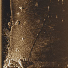
Ground-penetrating radar
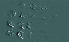
Contrary to conventional ground-penetrating radars, the one developed here uses a magnetic, not an electric field. In its current version, this means less but much more accessible information as the signal is less obscured by the small and natural variations in the ground, and instead reflects mainly from less abundant interfaces, such as those of buried objects. The system contains an antenna which transmits an electromagnetic wave with MHz frequency, and a magnetic field sensor (cf. SDTM project) which measures the standing waves resulting from interaction of the transmitted with the reflected wave. By using three orthogonal frequencies, the distance can be determined. Excluding the antenna, the system is about a cubic decimeter in size, which makes it suitable for field surveys. And indeed, some of the evaluation was made in the field. For instance, distance measurements were conducted through snow, which is an unwanted substance for conventional systems.
Project members: Anders Persson, Johan Sundqvist, Mikael Blomqvist, Tran Minh Nhut, Hugo Nguyen and Greger Thornell
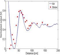 Signal vs snow depth in field measurements. |
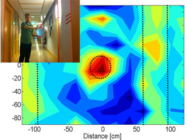 First attempt to map metallic objects indoors. (The metal plate as well as wall-embedded beams and air ducts are visible.) |